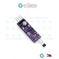
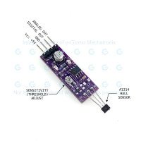
Analog Output: The exact analog output voltage range depends on the input supply voltage (Vcc) you provide to the module`s VCC pin. Because the A1314 is a ratiometric linear Hall effect sensor, its output characteristics scale directly with its supply voltage. 1. Quiescent Output Voltage (Zero Magnetic Field)
When there is no magnetic field present (0 Gauss), the analog output (Vout) rests at exactly half of the supply voltage:
Quiescent Vout = Vcc divided by 2 At 5.0V Supply: Resets to 2.50VAt 3.3V Supply: Resets to 1.65V 2. Full-Scale Analog Output Voltage Range
As a magnet approaches the sensor, the voltage will swing up or down from that middle resting point depending on the magnetic pole (North or South). The output architecture allows it to swing nearly rail-to-rail, typically within 0.2V to 0.4V of the supply limits under maximum magnetic saturation:
-
When powered at 5V: The analog output range is approximately 0.2V to 4.8V. --South Pole approaching: Voltage increases from 2.5V up toward roughly 4.8V. -- North Pole approaching: Voltage decreases from 2.5V down toward roughly 0.2V. When powered at 3.3V: The analog output range is approximately 0.2V to 3.1V.Summary Matrix for ADC Interfacing
-Powered at 5.0V --No Magnetic Field (0 G): roughly 2.5V --Max South Pole Saturation: roughly 4.7V to 4.8V --Max North Pole Saturation: roughly 0.2V to 0.3V -Powered at 3.3V --No Magnetic Field (0 G): roughly 1.65V --Max South Pole Saturation: roughly 3.0V to 3.1V --Max North Pole Saturation: roughly 0.2V to 0.3V Note: Since the output is linear and ratiometric, ensure your microcontroller`s ADC reference voltage (Vref) matches the Vcc supplying the module. This prevents slight fluctuations in your power rail from changing your magnetic field readings.
1
" aria-label="THEORY OF OPERATION: The e-Gizmo Vibration Sensor Module operates by processing the physical
mechanical state of the SW-18015P switch through an RC filter network and
an LM311 comparator stage: 1. Sensor Trigger & Signal Conditioning: - The SW-18015P sensor switch is connected across the input node (IN / Pin 3
of J1). Under resting conditions, the switch contact remains open.
- Upon physical vibration or impact, the internal spring element inside the
SW-18015P momentarily contacts the terminal wall, bringing the input
node low. - An RC filter composed of resistor R2 = 10 kOhm and capacitor C1 = 100 nF
filters noise spikes and smooths transient voltage swings before passing
the signal to the inverting input (Pin 2) of the LM311 comparator (U1). -The raw node voltage is routed directly to the ANA pin on connector J2.
Because the primary sensor is a mechanical on-off switch, the signal on
ANA consists of logic-level state transitions rather than a true
continuous variable voltage. 2. Voltage Comparison & Reference Threshold: - Resistors R1 = 10 kOhm and R4 = 10 kOhm form a precision fixed voltage
divider between Vcc and GND (RV1 is shorted across all terminals). This
establishes a stable reference voltage at the non-inverting input
(Pin 3 of LM311):
Vref = Vcc *R4 / (R1 + R4) = 1/2 Vcc (approx. 2.5V DC at +5V DC) -Power supply stability is maintained across the comparator via
decoupling capacitor C2 = 33 uF / 6V. 3. Digital Output & Indicator Logic: -The LM311 utilizes an open-collector output stage (Pin 7) pulled up to Vcc
by pull-up resistor R5 = 4.7 kOhm. - Quiescent State (No Vibration): The input voltage remains above Vref. The
LM311 output transistor remains OFF (high impedance), and R5 pulls the
DIG line to a logic HIGH state (+5V). The Red LED (D1) remains OFF. - Triggered State (Vibration Detected): When mechanical motion causes the
sensor contact to close, the voltage at input Pin 2 drops below Vref.
The LM311 output transistor turns ON, sinking current to Ground: - The DIG signal transitions to a logic LOW state (0V, Active Low). - Current flows through resistor R6 = 2.4 kOhm and the Red LED (D1),
driving D1 ON to indicate motion detection.
">
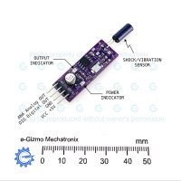
THEORY OF OPERATION: The e-Gizmo Vibration Sensor Module operates by processing the physical
mechanical state of the SW-18015P switch through an RC filter network and
an LM311 comparator stage: 1. Sensor Trigger & Signal Conditioning: - The SW-18015P sensor switch is connected across the input node (IN / Pin 3
of J1). Under resting conditions, the switch contact remains open.
- Upon physical vibration or impact, the internal spring element inside the
SW-18015P momentarily contacts the terminal wall, bringing the input
node low. - An RC filter composed of resistor R2 = 10 kOhm and capacitor C1 = 100 nF
filters noise spikes and smooths transient voltage swings before passing
the signal to the inverting input (Pin 2) of the LM311 comparator (U1). -The raw node voltage is routed directly to the ANA pin on connector J2.
Because the primary sensor is a mechanical on-off switch, the signal on
ANA consists of logic-level state transitions rather than a true
continuous variable voltage. 2. Voltage Comparison & Reference Threshold: - Resistors R1 = 10 kOhm and R4 = 10 kOhm form a precision fixed voltage
divider between Vcc and GND (RV1 is shorted across all terminals). This
establishes a stable reference voltage at the non-inverting input
(Pin 3 of LM311):
Vref = Vcc *R4 / (R1 + R4) = 1/2 Vcc (approx. 2.5V DC at +5V DC) -Power supply stability is maintained across the comparator via
decoupling capacitor C2 = 33 uF / 6V. 3. Digital Output & Indicator Logic: -The LM311 utilizes an open-collector output stage (Pin 7) pulled up to Vcc
by pull-up resistor R5 = 4.7 kOhm. - Quiescent State (No Vibration): The input voltage remains above Vref. The
LM311 output transistor remains OFF (high impedance), and R5 pulls the
DIG line to a logic HIGH state (+5V). The Red LED (D1) remains OFF. - Triggered State (Vibration Detected): When mechanical motion causes the
sensor contact to close, the voltage at input Pin 2 drops below Vref.
The LM311 output transistor turns ON, sinking current to Ground: - The DIG signal transitions to a logic LOW state (0V, Active Low). - Current flows through resistor R6 = 2.4 kOhm and the Red LED (D1),
driving D1 ON to indicate motion detection.
1
" aria-label="THEORY OF OPERATION 1. Photoresistor (LDR) & Analog Signal Generation The sensing element is a Cadmium Sulfide (CdS) Light Dependent Resistor connected across J1 Pin 3 (IN) and GND. It forms a voltage divider circuit with fixed resistor R2 (10 k-ohms), which is pulled up to VCC (+5V). The resulting analog voltage V_ANA at node IN is given by: V_ANA = VCC * (R_LDR / (R2 + R_LDR)) - Dark Environment:
R_LDR is extremely high (typically greater than or equal to 1 M-ohm). Because R_LDR is much greater than R2, the voltage V_ANA remains high, close to VCC (+5V). - Bright Environment:
R_LDR drops significantly (typically 1 k-ohm - 10 k-ohms). As R_LDR decreases relative to R2 = 10 k-ohms, V_ANA falls towards ground (0V). Filter capacitor C1 (100 nF) is connected in parallel across the LDR to ground, smoothing rapid light fluctuations and removing high-frequency electrical noise from V_ANA. This signal is exposed on J2 Pin 1 (ANA) for direct measurement by microcontroller ADCs. 2. Threshold Reference Voltage Generation A stable comparison threshold voltage V_ref is established using a resistive divider network comprising R1 (1 k-ohm), trimmer potentiometer RV1 (6.8 k-ohms), and R4 (1 k-ohm) connected between VCC and GND: V_ref(min) = VCC * (R4 / (R1 + RV1 + R4)) = 5V * (1 k-ohm / 8.8 k-ohms) = approx. 0.57V V_ref(max) = VCC * ((RV1 + R4) / (R1 + RV1 + R4)) = 5V * (7.8 k-ohms / 8.8 k-ohms) = approx. 4.43V Adjusting RV1 allows precise tuning of V_ref at Pin 3 (non-inverting input V+) of the LM311 comparator (U1). 3. Digital Switching via LM311 Comparator The LM311 comparator (U1) continuously compares the filtered analog sensor voltage V_ANA at Pin 2 (inverting input V-) against reference voltage V_ref at Pin 3 (non-inverting input V+). a. Dark / Below-Threshold Condition (V_ANA > V_ref): -V- (Pin 2) is higher than V+ (Pin 3). - The LM311 internal output transistor remains OFF (open-collector). - Resistor R5 (4.7 k-ohms) pulls Pin 7 (DIG) HIGH to VCC (+5V). - Red LED D1 remains OFF because there is no ground path through Pin 7. b. Bright / Threshold Reached Condition (V_ANA <= V_ref): - As ambient brightness increases, R_LDR drops and V_ANA falls below V_ref. - V- (Pin 2) becomes less than or equal to V+ (Pin 3). - The LM311 output transistor turns ON, pulling Pin 7 (DIG) LOW to 0V. - Current flows from VCC through R6 (2.4 k-ohms) and Red LED D1 into Pin 7 to ground, illuminating D1. - The DIGITAL OUT pin (J2 Pin 2) provides a clean Active-LOW logic output (0V).
">
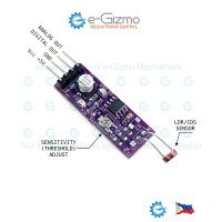
THEORY OF OPERATION 1. Photoresistor (LDR) & Analog Signal Generation The sensing element is a Cadmium Sulfide (CdS) Light Dependent Resistor connected across J1 Pin 3 (IN) and GND. It forms a voltage divider circuit with fixed resistor R2 (10 k-ohms), which is pulled up to VCC (+5V). The resulting analog voltage V_ANA at node IN is given by: V_ANA = VCC * (R_LDR / (R2 + R_LDR)) - Dark Environment:
R_LDR is extremely high (typically greater than or equal to 1 M-ohm). Because R_LDR is much greater than R2, the voltage V_ANA remains high, close to VCC (+5V). - Bright Environment:
R_LDR drops significantly (typically 1 k-ohm - 10 k-ohms). As R_LDR decreases relative to R2 = 10 k-ohms, V_ANA falls towards ground (0V). Filter capacitor C1 (100 nF) is connected in parallel across the LDR to ground, smoothing rapid light fluctuations and removing high-frequency electrical noise from V_ANA. This signal is exposed on J2 Pin 1 (ANA) for direct measurement by microcontroller ADCs. 2. Threshold Reference Voltage Generation A stable comparison threshold voltage V_ref is established using a resistive divider network comprising R1 (1 k-ohm), trimmer potentiometer RV1 (6.8 k-ohms), and R4 (1 k-ohm) connected between VCC and GND: V_ref(min) = VCC * (R4 / (R1 + RV1 + R4)) = 5V * (1 k-ohm / 8.8 k-ohms) = approx. 0.57V V_ref(max) = VCC * ((RV1 + R4) / (R1 + RV1 + R4)) = 5V * (7.8 k-ohms / 8.8 k-ohms) = approx. 4.43V Adjusting RV1 allows precise tuning of V_ref at Pin 3 (non-inverting input V+) of the LM311 comparator (U1). 3. Digital Switching via LM311 Comparator The LM311 comparator (U1) continuously compares the filtered analog sensor voltage V_ANA at Pin 2 (inverting input V-) against reference voltage V_ref at Pin 3 (non-inverting input V+). a. Dark / Below-Threshold Condition (V_ANA > V_ref): -V- (Pin 2) is higher than V+ (Pin 3). - The LM311 internal output transistor remains OFF (open-collector). - Resistor R5 (4.7 k-ohms) pulls Pin 7 (DIG) HIGH to VCC (+5V). - Red LED D1 remains OFF because there is no ground path through Pin 7. b. Bright / Threshold Reached Condition (V_ANA <= V_ref): - As ambient brightness increases, R_LDR drops and V_ANA falls below V_ref. - V- (Pin 2) becomes less than or equal to V+ (Pin 3). - The LM311 output transistor turns ON, pulling Pin 7 (DIG) LOW to 0V. - Current flows from VCC through R6 (2.4 k-ohms) and Red LED D1 into Pin 7 to ground, illuminating D1. - The DIGITAL OUT pin (J2 Pin 2) provides a clean Active-LOW logic output (0V).
1
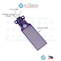
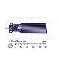
- Liquid Conductivity: When dry, the air acts as an insulator, creating an open circuit (extremely high resistance) between adjacent traces. When submerged, the water bridges the gap between these interleaved traces. Because typical water contains dissolved ions, it conducts electricity. 2. Resistance vs. Water Level - Deep Submersion = Lower Resistance: As the water level rises, a larger surface area of the traces is submerged. This provides more parallel conductive paths for current to flow through the liquid, which decreases the overall electrical resistance between the traces. - Shallow Submersion = Higher Resistance: When the water level is low, fewer paths are available, resulting in a higher electrical resistance. 3. Signal Conditioning and Output - Voltage Divider/Amplifier Circuit: The onboard components—including the transistor (Q1), resistors, and capacitor—form a basic signal-conditioning circuit (often a voltage divider or an emitter-follower amplifier). - Analog Voltage Output: This circuit converts the shifting resistance of the sensing pads into a proportional analog voltage at the S pin: -- Dry / Low Level: Lower voltage output (near 0V). -- High Level: Higher voltage output (approaching the +3 to 5VDC supply voltage).Note: Because this sensor relies on direct electrical contact with water, it is highly susceptible to electrolysis and corrosion over time if powered continuously. To extend its lifespan in practical applications, it is best to only apply power to the (+) pin right before taking a measurement, and turn it off immediately after.
" aria-label="Theory of Operation: Resistive Water Level Sensor This module functions as a variable resistor that changes its resistance based on its depth of immersion in a conductive liquid (like tap water). 1. The Sensing Mechanism - Interleaved Traces: The "Sensing Area" consists of alternating, parallel conductive traces exposed on the PCB. One set of traces is connected to the supply voltage (+), and the adjacent interleaved set is connected to the signal conditioning circuit. - Liquid Conductivity: When dry, the air acts as an insulator, creating an open circuit (extremely high resistance) between adjacent traces. When submerged, the water bridges the gap between these interleaved traces. Because typical water contains dissolved ions, it conducts electricity. 2. Resistance vs. Water Level - Deep Submersion = Lower Resistance: As the water level rises, a larger surface area of the traces is submerged. This provides more parallel conductive paths for current to flow through the liquid, which decreases the overall electrical resistance between the traces. - Shallow Submersion = Higher Resistance: When the water level is low, fewer paths are available, resulting in a higher electrical resistance. 3. Signal Conditioning and Output - Voltage Divider/Amplifier Circuit: The onboard components—including the transistor (Q1), resistors, and capacitor—form a basic signal-conditioning circuit (often a voltage divider or an emitter-follower amplifier). - Analog Voltage Output: This circuit converts the shifting resistance of the sensing pads into a proportional analog voltage at the S pin: -- Dry / Low Level: Lower voltage output (near 0V). -- High Level: Higher voltage output (approaching the +3 to 5VDC supply voltage).Note: Because this sensor relies on direct electrical contact with water, it is highly susceptible to electrolysis and corrosion over time if powered continuously. To extend its lifespan in practical applications, it is best to only apply power to the (+) pin right before taking a measurement, and turn it off immediately after.
">
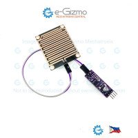
Theory of Operation: Resistive Water Level Sensor This module functions as a variable resistor that changes its resistance based on its depth of immersion in a conductive liquid (like tap water). 1. The Sensing Mechanism - Interleaved Traces: The "Sensing Area" consists of alternating, parallel conductive traces exposed on the PCB. One set of traces is connected to the supply voltage (+), and the adjacent interleaved set is connected to the signal conditioning circuit. - Liquid Conductivity: When dry, the air acts as an insulator, creating an open circuit (extremely high resistance) between adjacent traces. When submerged, the water bridges the gap between these interleaved traces. Because typical water contains dissolved ions, it conducts electricity. 2. Resistance vs. Water Level - Deep Submersion = Lower Resistance: As the water level rises, a larger surface area of the traces is submerged. This provides more parallel conductive paths for current to flow through the liquid, which decreases the overall electrical resistance between the traces. - Shallow Submersion = Higher Resistance: When the water level is low, fewer paths are available, resulting in a higher electrical resistance. 3. Signal Conditioning and Output - Voltage Divider/Amplifier Circuit: The onboard components—including the transistor (Q1), resistors, and capacitor—form a basic signal-conditioning circuit (often a voltage divider or an emitter-follower amplifier). - Analog Voltage Output: This circuit converts the shifting resistance of the sensing pads into a proportional analog voltage at the S pin: -- Dry / Low Level: Lower voltage output (near 0V). -- High Level: Higher voltage output (approaching the +3 to 5VDC supply voltage).Note: Because this sensor relies on direct electrical contact with water, it is highly susceptible to electrolysis and corrosion over time if powered continuously. To extend its lifespan in practical applications, it is best to only apply power to the (+) pin right before taking a measurement, and turn it off immediately after.
1
" aria-label="Theory of Operation 1. Resistive Rain Sensing PCB The external sensor board consists of two set sets of exposed, interleaved nickel/copper traces. * Dry State: Air acts as an insulator between the traces, creating a very high resistance across the sensor terminals (J1 IN to GND). * Wet State: Water droplet accumulation acts as a conductive bridge across the traces, significantly decreasing resistance proportionally to the amount of liquid bridging the gap. 2. Analog Output (ANA) The rain board forms a voltage divider circuit with onboard resistors (R1, R2). As water contacts the sensor pad and decreases its resistance, the node voltage directly reflects this change. This variable voltage signal is routed straight to the ANA output pin, allowing microcontrollers to read analog values (via ADC) to estimate rainfall intensity or surface wetness levels. 3. Comparator & Digital Output (DIG) The module utilizes an LM311 voltage comparator to generate a clean, chatter-free digital threshold output: * A reference voltage is set at the non-inverting input (V+) using the onboard trimpot (RV1). * The variable sensor voltage from the rain pad is fed into the inverting input (V−). * When dry, V− remains higher than V+, keeping the comparator output High-Z/pulled HIGH (Normally HIGH). * When raindrops lower the sensor resistance, V− drops below V+. The LM311 pulls the output pin (DIG) LOW to ground, simultaneously turning on the red OUTPUT INDICATOR LED (D1) to signal wet conditions.
">
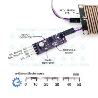
Theory of Operation 1. Resistive Rain Sensing PCB The external sensor board consists of two set sets of exposed, interleaved nickel/copper traces. * Dry State: Air acts as an insulator between the traces, creating a very high resistance across the sensor terminals (J1 IN to GND). * Wet State: Water droplet accumulation acts as a conductive bridge across the traces, significantly decreasing resistance proportionally to the amount of liquid bridging the gap. 2. Analog Output (ANA) The rain board forms a voltage divider circuit with onboard resistors (R1, R2). As water contacts the sensor pad and decreases its resistance, the node voltage directly reflects this change. This variable voltage signal is routed straight to the ANA output pin, allowing microcontrollers to read analog values (via ADC) to estimate rainfall intensity or surface wetness levels. 3. Comparator & Digital Output (DIG) The module utilizes an LM311 voltage comparator to generate a clean, chatter-free digital threshold output: * A reference voltage is set at the non-inverting input (V+) using the onboard trimpot (RV1). * The variable sensor voltage from the rain pad is fed into the inverting input (V−). * When dry, V− remains higher than V+, keeping the comparator output High-Z/pulled HIGH (Normally HIGH). * When raindrops lower the sensor resistance, V− drops below V+. The LM311 pulls the output pin (DIG) LOW to ground, simultaneously turning on the red OUTPUT INDICATOR LED (D1) to signal wet conditions.
1
" aria-label="Theory of Operation This compact module is designed for precise, isolated AC, DC, or pulsed current measurement. Below is a breakdown of how the circuit and its primary component, the LEM HLSR 50-P, operate. 1. Core Sensor Technology (U1)
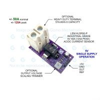
At the heart of the module is U1, the LEM HLSR 50-P current transducer. -Hall-Effect Transduction: It operates on the open-loop Hall-effect principle. When current passes through the primary circuit via the terminal block (J2), it flows through internal bus bars connected to pins IN1+/IN2+ and IN1-/IN2-. -Magnetic Coupling: This current generates a magnetic field proportional to its magnitude. A high-bandwidth, low-loss magnetic core inside the IC concentrates this field onto an internal Hall-effect plate. - Galvanic Isolation: Because the primary current only couples magnetically to the internal sensor, there is complete physical and electrical (galvanic) separation between the high-power input path (J2) and the low-voltage control electronics (J1). 2. Signal Generation & Referencing
- Ratiometric Voltage Output (Uout): The transducer outputs an analog voltage on pin 2 (Uout) that tracks the measured primary current.
-
Reference Voltage (Uref): Under zero-current conditions, the sensor outputs a stable reference voltage at pin 1 (Uref), which typically sits at half the supply voltage (e.g., 2.5 V when powered by a +5 V rail). As current flows in a positive or negative direction, Uout swings linearly above or below this Uref level -.Filtering: Capacitors C1, C2, and C3 (100 nF) act as decoupling and bypass elements for the sensitive Uout and Uref lines to suppress high-frequency noise. 3. Scale Calibration & Readout Interface (RV1 & JP1)
The module features a highly versatile scaling network at its output stage: -The Scaling Network: A 100 kOhm multi-turn trimpot (RV1) is connected directly between the output (Uout) and the reference (Uref). - Adjustable Output vs. Direct Pass-Through: -- When JP1 is open (not shorted): The output signal fed to the header pin OUT (J1, pin 3) is tapped from the wiper of RV1. This allows you to scale the sensor's raw sensitivity (e.g., matching a default 16 mV/A down to 10 mV/A). This calibrated output is ideal when reading the signal directly with a Digital Multimeter (DMM), as it translates directly to round-number scale factors. -- When JP1 is shorted: The trimpot RV1 is bypassed, routing the raw, unattenuated output (Uout) directly to the OUT terminal of header J1. -Filter Capacitor (C4): A 33uF capacitor (C4) stabilizes the output, filtering ripple and low-frequency noise for cleaner micro-controller or multimeter ADC reads. 4. Power Supply & Indication
Power Input: The module operates on a single +5 V supply fed through pins 1 (+5V) and 2 (GND) of header J1. 5. Schematic Diagram
">
Theory of Operation This compact module is designed for precise, isolated AC, DC, or pulsed current measurement. Below is a breakdown of how the circuit and its primary component, the LEM HLSR 50-P, operate. 1. Core Sensor Technology (U1)
At the heart of the module is U1, the LEM HLSR 50-P current transducer. -Hall-Effect Transduction: It operates on the open-loop Hall-effect principle. When current passes through the primary circuit via the terminal block (J2), it flows through internal bus bars connected to pins IN1+/IN2+ and IN1-/IN2-. -Magnetic Coupling: This current generates a magnetic field proportional to its magnitude. A high-bandwidth, low-loss magnetic core inside the IC concentrates this field onto an internal Hall-effect plate. - Galvanic Isolation: Because the primary current only couples magnetically to the internal sensor, there is complete physical and electrical (galvanic) separation between the high-power input path (J2) and the low-voltage control electronics (J1). 2. Signal Generation & Referencing
- Ratiometric Voltage Output (Uout): The transducer outputs an analog voltage on pin 2 (Uout) that tracks the measured primary current.
-
Reference Voltage (Uref): Under zero-current conditions, the sensor outputs a stable reference voltage at pin 1 (Uref), which typically sits at half the supply voltage (e.g., 2.5 V when powered by a +5 V rail). As current flows in a positive or negative direction, Uout swings linearly above or below this Uref level -.Filtering: Capacitors C1, C2, and C3 (100 nF) act as decoupling and bypass elements for the sensitive Uout and Uref lines to suppress high-frequency noise. 3. Scale Calibration & Readout Interface (RV1 & JP1)
The module features a highly versatile scaling network at its output stage: -The Scaling Network: A 100 kOhm multi-turn trimpot (RV1) is connected directly between the output (Uout) and the reference (Uref). - Adjustable Output vs. Direct Pass-Through: -- When JP1 is open (not shorted): The output signal fed to the header pin OUT (J1, pin 3) is tapped from the wiper of RV1. This allows you to scale the sensor's raw sensitivity (e.g., matching a default 16 mV/A down to 10 mV/A). This calibrated output is ideal when reading the signal directly with a Digital Multimeter (DMM), as it translates directly to round-number scale factors. -- When JP1 is shorted: The trimpot RV1 is bypassed, routing the raw, unattenuated output (Uout) directly to the OUT terminal of header J1. -Filter Capacitor (C4): A 33uF capacitor (C4) stabilizes the output, filtering ripple and low-frequency noise for cleaner micro-controller or multimeter ADC reads. 4. Power Supply & Indication
Power Input: The module operates on a single +5 V supply fed through pins 1 (+5V) and 2 (GND) of header J1. 5. Schematic Diagram
2
" aria-label="Theory of Operation This compact module is designed for precise, isolated AC, DC, or pulsed current measurement. Below is a breakdown of how the circuit and its primary component, the LEM HLSR 50-P, operate. 1. Core Sensor Technology (U1)
At the heart of the module is U1, the LEM HLSR 50-P current transducer. -Hall-Effect Transduction: It operates on the open-loop Hall-effect principle. When current passes through the primary circuit via the terminal block (J2), it flows through internal bus bars connected to pins IN1+/IN2+ and IN1-/IN2-. -Magnetic Coupling: This current generates a magnetic field proportional to its magnitude. A high-bandwidth, low-loss magnetic core inside the IC concentrates this field onto an internal Hall-effect plate. - Galvanic Isolation: Because the primary current only couples magnetically to the internal sensor, there is complete physical and electrical (galvanic) separation between the high-power input path (J2) and the low-voltage control electronics (J1). 2. Signal Generation & Referencing
- Ratiometric Voltage Output (Uout): The transducer outputs an analog voltage on pin 2 (Uout) that tracks the measured primary current.
-
Reference Voltage (Uref): Under zero-current conditions, the sensor outputs a stable reference voltage at pin 1 (Uref), which typically sits at half the supply voltage (e.g., 2.5 V when powered by a +5 V rail). As current flows in a positive or negative direction, Uout swings linearly above or below this Uref level -.Filtering: Capacitors C1, C2, and C3 (100 nF) act as decoupling and bypass elements for the sensitive Uout and Uref lines to suppress high-frequency noise. 3. Scale Calibration & Readout Interface (RV1 & JP1)
The module features a highly versatile scaling network at its output stage: -The Scaling Network: A 100 kOhm multi-turn trimpot (RV1) is connected directly between the output (Uout) and the reference (Uref). - Adjustable Output vs. Direct Pass-Through: -- When JP1 is open (not shorted): The output signal fed to the header pin OUT (J1, pin 3) is tapped from the wiper of RV1. This allows you to scale the sensor's raw sensitivity (e.g., matching a default 16 mV/A down to 10 mV/A). This calibrated output is ideal when reading the signal directly with a Digital Multimeter (DMM), as it translates directly to round-number scale factors. -- When JP1 is shorted: The trimpot RV1 is bypassed, routing the raw, unattenuated output (Uout) directly to the OUT terminal of header J1. -Filter Capacitor (C4): A 33uF capacitor (C4) stabilizes the output, filtering ripple and low-frequency noise for cleaner micro-controller or multimeter ADC reads. 4. Power Supply & Indication
Power Input: The module operates on a single +5 V supply fed through pins 1 (+5V) and 2 (GND) of header J1. 5. Schematic Diagram
">
Theory of Operation This compact module is designed for precise, isolated AC, DC, or pulsed current measurement. Below is a breakdown of how the circuit and its primary component, the LEM HLSR 50-P, operate. 1. Core Sensor Technology (U1)
At the heart of the module is U1, the LEM HLSR 50-P current transducer. -Hall-Effect Transduction: It operates on the open-loop Hall-effect principle. When current passes through the primary circuit via the terminal block (J2), it flows through internal bus bars connected to pins IN1+/IN2+ and IN1-/IN2-. -Magnetic Coupling: This current generates a magnetic field proportional to its magnitude. A high-bandwidth, low-loss magnetic core inside the IC concentrates this field onto an internal Hall-effect plate. - Galvanic Isolation: Because the primary current only couples magnetically to the internal sensor, there is complete physical and electrical (galvanic) separation between the high-power input path (J2) and the low-voltage control electronics (J1). 2. Signal Generation & Referencing
- Ratiometric Voltage Output (Uout): The transducer outputs an analog voltage on pin 2 (Uout) that tracks the measured primary current.
-
Reference Voltage (Uref): Under zero-current conditions, the sensor outputs a stable reference voltage at pin 1 (Uref), which typically sits at half the supply voltage (e.g., 2.5 V when powered by a +5 V rail). As current flows in a positive or negative direction, Uout swings linearly above or below this Uref level -.Filtering: Capacitors C1, C2, and C3 (100 nF) act as decoupling and bypass elements for the sensitive Uout and Uref lines to suppress high-frequency noise. 3. Scale Calibration & Readout Interface (RV1 & JP1)
The module features a highly versatile scaling network at its output stage: -The Scaling Network: A 100 kOhm multi-turn trimpot (RV1) is connected directly between the output (Uout) and the reference (Uref). - Adjustable Output vs. Direct Pass-Through: -- When JP1 is open (not shorted): The output signal fed to the header pin OUT (J1, pin 3) is tapped from the wiper of RV1. This allows you to scale the sensor's raw sensitivity (e.g., matching a default 16 mV/A down to 10 mV/A). This calibrated output is ideal when reading the signal directly with a Digital Multimeter (DMM), as it translates directly to round-number scale factors. -- When JP1 is shorted: The trimpot RV1 is bypassed, routing the raw, unattenuated output (Uout) directly to the OUT terminal of header J1. -Filter Capacitor (C4): A 33uF capacitor (C4) stabilizes the output, filtering ripple and low-frequency noise for cleaner micro-controller or multimeter ADC reads. 4. Power Supply & Indication
Power Input: The module operates on a single +5 V supply fed through pins 1 (+5V) and 2 (GND) of header J1. 5. Schematic Diagram
1