


-50x50w.jpg "gizDuino + with ATmega324")


LCMX02 FPGA Breakout Board Quick Start Guide (VHDL examples)
")
Our new FPGA’s (Field Programmable Gate Arrays):

LCMX02 FPGA Breakout Board Hardware Manual
Look at our new e-Gizmo FPGA LCMX02 Breakout Board.
On this short video, it shows you the output after the program successfully uploaded to the board.
Materials Needed:
Diamond Base Software Downloads:
Important Requirements! Your Operating System must be 64-bit
Lattice Diamond Download
-Full featured VHDL/Verlog IDE with simulator. “Registration required, but it’s totally free. “
Windows
Choose the 1.6 GB size and 3.10 version

Troubleshoot: If there’s an error when you open the Lattice Diamond. Kindly go to this link and follow the instructions carefully.
1 . Go to Lattice Diamond Development Suite. Click the Licensing, you need this to use the software.

b. Then Scroll-down and look for Lattice Diamond Free License, and Click “Request a Free License”

c. Just follow these steps for requesting your free license.

DONE! You can now use the Software..,
Next On how to upload program on the board.
Connections:
LED (+) --> L5B

LED (-) --> GND

Procedure:
a. Open the Lattice Diamond 3.10. On the Start Page> Project>Click New…
or File>New>Project…
Name: LED_Blinking
Location: Click Browse. (Mine i have Lattice Workspace folder on my Desktop)

a.1 Create New Folder > LED_Blinking (Then Select it)

Then Click Next!
b. On the add source/Sources file. Click Next.

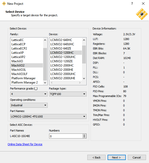
c. Select Device.
Family: MachXO2
Device: LCMXO2-1200HC
Performance grade: 4
Package type: TQFP100
Operating conditions: Industrial
Part Names: LCMXO2-1200HC-4TG100I
d. On the Syhthesis Tools, Click Next.

e. On the Project Information, Click Next.

f. The LED_Blinking project summary will show (Reports)

Create New File
- Go to File> New > File…

2. Select the Source Files> VHDL Files, Name: LED_Blinking, Select the correct location.

3. A New tab will show.

Code
Copy & Paste this code.

After that Go to Process section (located at left side), Double-Click the Synthesize Design. Then Click OK.


SPREADSHEETS
Go to tools, select the Spreadsheet.

On this view, go to row 1.1.1 and Pin Column. Type the PL5B (Pin 13 on the IC)

Next, On the Process Select the Map Trace, Place & Route Trace, I/O Timing Analysis, Bitstream File, JEDEC File.

Export Files, Then OK.

After Exported the files,

See if all the selected file on the process has passed and then you may proceed.
PROGRAMMER
Go to Tools> Programmer

Click the Detect Cable, Make sure you’ve plug in the FT2232 breakout kit with FPGA LCMXO2 Breakout board.

Select the USB2 -FTUSB-1 (Dual RS232-HS A Location 0001).

(Consistently) Select the Device
The device section will turn Yellow Color, and there’s a WARNING on the Output Terminal
WARNING – Cannot identify detected device on row 1. Please manually select the correct device.


OPERATION
Select the Device Operation you want to use.
- Flash Programming Mode
- Static RAM Cell Mode (This one i used)
Access mode:

Operation:

Programming Options> Programming file
Select the (.bit) file.


Once the the Device Properties is set. Click OK.
PROGRAM
Click the Program ICON.

Starting "pgr_program run"
Wait Until the Operation: Successful.

The STATUS is PASS!

and your LED on the FPGA board will blink.
For more information about FPGA Blinking LED (see below the link)
Reference:
Philippine Electronics Forum
Leave a Comment